I was looking at the same image.
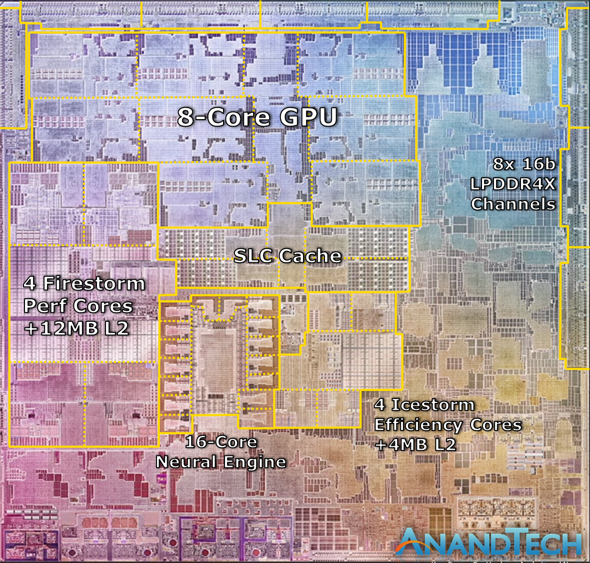
A very large part of the die is not labelled and it must include some blocks that cannot be omitted from the CPU, e.g. the PCIe controller and various parts from the memory controller, e.g. buffers and prefetchers.
The area labelled for the memory channels seems to contain just the physical interfaces for the memory, that is why it is small. The complete memory controller must include parts of the unlabelled area.
Even if the CPU part of M1 would be smaller, e.g. just a quarter, that would be 30 square mm. In the 32 nm technology that would likely need much more than 1000 square mm, i.e. it would be impossible to be manufactured.
The number of transistors claimed for various CPUs or GPUs is mostly meaningless and usually very far from the truth anyway.
The only thing that matters for estimating the costs and the scaling to other processes is the area occupied on the die, which is determined by much more factors than the number of transistors used, even if that would have been reported accurately. (The transistors are not identical, they can have very different sizes and the area of various parts of a CPU may be determined more by the number of interconnections than by the number of transistors.)