https://en.wikipedia.org/wiki/Chiplet
This seems to be about the third reason listed:
> Known good die (KGD): chiplets can be tested before assembly, improving the yield of the final device
Problem:
  > In general, a killer defect is defined as a defect that is 20% the size of the fabrication node.  For
  > example, a defect that is less than 9nm may be acceptable for the 45nm fabrication node, but a defect
  > larger than 2.8nm would be defined as a “killer” defect for the 14nm fabrication node.  For the 5nm
  > fabrication node, a defect measuring only 1nm could be a killer.
  >
  > This is one of the primary reasons that it has become increasingly difficult to yield large monolithic
  > ICs (as measured in die area) when using leading edge fabrication process technology
https://www.nextplatform.com/2021/06/09/amd-on-why-chiplets-...
https://cdn.wccftech.com/wp-content/uploads/2018/11/AMD-EPYC...
Because a vacuum pretty eliminates dust - with no air, dust just falls towards either the ground (if it is uncharged), or towards a positive or negatively charged surface (if the dust particle itself is charged).
Until 2005 or so, shrinking transistors automatically increased speed and reduced power consumption. When that ran out of steam, the industry went to multi core and massive parallelism with GPUs.
Until recently each shrink also lowered the cost per transistor, but that seems to have run out also and has something to do with why Intel was stuck at 14nm for so long and why new GPU prices are so insane despite a collapse in demand and resolution of the supply chain crisis for high end chips.
Chiplets at best are neutral with regard to cost. If manufacturing overhead is low, two chiplets give you twice the transistors at twice the cost. The industry did not pursue chiplets with a lot of vigor until now because it was a less competitive approach to scaling than shrinking transistors until now.
That business plan is no longer functional for Intel. Translated, Moore's business plan was to shrink die size, and speed up clocks, so much as to obsolete their previous offering with an 18 month half life.
It just doesn't work that way anymore, and hasn't for quite some time.
Engelbart's Scaling Observation[0], on the other hand, remains quite interesting, and from what I see remains in force. Genetics in particular is still pulling exponential gains out of the luminiferous ether.
So everyone that works in other domains, without access to libraries written by the GPU druids, largely ignores their existence.
Consumer machines vary wildly in their GPU capabilities, especially VRAM. So how do you know that your nice accelerated algorithm is going to work if the user has an old GPU? And what do you do if it doesn’t work? Run on the CPU? Tell the user their machine is too weak?
Here the advantage of GPUs (performance) is also the biggest disadvantage: a gigantic range of performance profiles. At least with CPUs the oldest CPU is only going to be a small integer factor slower than a new one in single thread.
What unites gamers and machine learning is an expectation that the user has a reasonably recent and capable GPU. But these are small, self-selecting populations.
On the server side the issue is cost. GPUs are expensive, and usually not necessary, so nobody is going to write code that requires one without a good reason.
That cost about the same as a single mid-range video card. (Nvidia RTX 3070)
Why on earth would you add a requirement to your software/workflow that doubles your cost, and is just about impossible to find in stock?
However they failed to implement with good results the methods that they had hoped to work, while the others, i.e. TSMC and Samsung had much more realistic roadmaps, which added EUV at the right moment.
Intel was not stalled by waiting for EUV, on the contrary they were not prepared for the transition that was necessary when EUV was eventually ready.
https://www.theverge.com/2022/10/4/23385652/pat-gelsinger-in...
If progress continues then they will need some other expensive machine. Either that or they’ll try to stretch the life of EUV the same way Intel tried to delay EUV with extreme multiple patterning.
It seems to me though that the ASML machines ought to get some competition from something more like a free electron laser.
That doesn't take into account yields. One chip with twice the transistors is physically larger than two chips with half as many, and more likely to have a defect during production.
> However, as it has in the past, the semiconductor ecosystem is adapting and as Chiplet technology builds traction, we will very likely see a period of accelerating innovation and new market opportunities opening as we move forward.
The whole premise is that chip innovation (and overall computing power) is continuing to accelerate, even though "Moore's Law as we've known it" has ended
Especially in the startup space I saw companies building software with the hypothesis “users need the latest device for our product and they will get faster anyway so we don’t need optimize our code. Instead we deliver features on max speed skipping optimizations and wait until our users upgraded to newer devices during the coming 2-4 years”.
I don’t even blame the companies for doing this. The benefit to cost ratio of using idk C++ for everything is just too bad.
https://www.cpubenchmark.net/singleThread.html
It's amazing how often this is parroted. Anyone with a passing familiarity with the numbers knows this is actually not true at all.
Better caching, branch prediction, plus vast amounts of SRAM. There's been a slow & steady increase in the vast variety of single threaded workloads grouped together by "instructions per clock."
Both at the peak of the voltage frequency curve for workstations & overclocking, the apex of the optimization curve for data centre, and especially at the bare minimum for mobile devices with idle workloads.
Yes, it's a small fraction of the old days. It's still double in 10 years.
And as anyone who's migrated from an Intel Mac to Apple Silicon knows, "merely doubling" is a LOT.
4.5 years later and Intel is bragging that their upcoming topline CPU will run 6GHz stock. I suppose one could call this a plateau compared to the good old days of the 80s and 90s, but it’s definitely still progress.
In late 2000, Intel promised that Pentium 4s will hit 10GHz by 2005 – on a presumed 130W power budget –, after the last 5 years saw clock speeds increase from 150MHz to 1.4GHz for the P6 architecture (at a stable 30-40W power budget), and other vendors saw similar increases.
Over 20 years later, we're barely scratching the 6GHz barrier with an opportunistic turbo mode that isn't guaranteed to kick in, if your cooling isn't up to the task of dissipating a record-breaking 250W of peak power consumption.
Pentium 4 HT 3.8F, November 2004, 3.8GHz, 115W TDP
Core i9-13900KF, October 2022, 3.0GHz, 125W TDP
Of course, the latter does give you 8 performance cores and 16 efficiency cores so performance-per-watt has clearly improved; and it has 'turbo boost'. But in terms of sustained single-core performance? It's clear Intel's attention has been elsewhere. Such as on the laptop market, where power efficiency is king.
and fwiw ive had a 5ghz+ overclock on every cpu ive bought in the last ten years with a corsair 240mm aio, going back to the 3570k
It's at least enough that we have to take it into account:
We run our workloads across multiple Intel cpu generations and to be able to optimize utilization we have a "speedup factor" which is currently up to 1.7 for the latest generation we've tuned it for. And the base 1.0 performance is from Ivy Bridge, launched 2013.
It was basically a monopolistic warning from one of the founders not to release new products too fast so the company wouldn’t burn out. It worked. But it’s not some scientific or physical law and I hate when people refer to it as such.
According to the article, Moore's Law predates the founding of Intel by several years.
Not about transistor size of performance.
So it was an economic insight, more than anything else.
Moving to chiplets doesn’t change transistor density. This is a packaging feature and not a fabrication feature. This is done for manufacturing cost reduction and yield improvements.
Transistor density doubling every 18 months for a similar cost.
https://t7m8e9c8.rocketcdn.me/wp-content/uploads/2020/09/pre...
https://en.wikipedia.org/wiki/Moore%27s_law#cite_note-Moore_...
By those terms, Moore's law is totally extinct.
Folk haven't noticed however, because the "leading edge" logic manufacturers have 60% gross margins. The vast majority of their costs are in design, distribution and overhead.
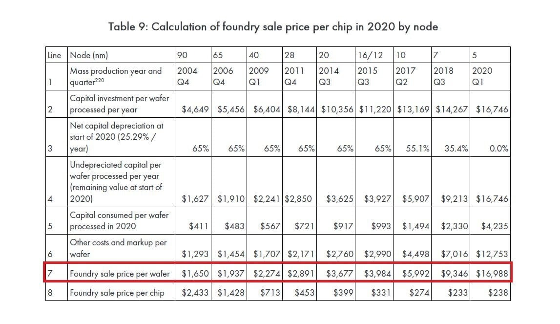
Price rises of 30% to 100% have disguised that the cost of manufacturing the silicon is an order of magnitude more than a decade ago.
Granted, the above numbers are not the actual inflation adjusted wafer cost for leading edge nodes.
But, $16,000 for a 300mm wafer is extraordinary.
I am no silicon engineer but I suspect a chip that fully takes advantage of the third dimension would be something like a sponge full of built in channels for the working fluid to remove heat.
First however I suspect you will see chiplets arranged vertically like heatsink fins and the whole cpu would effectively be the water block, basically a vlsi version of the cray 3
What you're describing is called 3D stacking, and it works.
It's just extraordinarily complex to resolve the intra-die latency issues, and many others, when going vertical. Hence expensive.
3D is also used in AMD's 3D cache.
But 3D logic on logic is more complicated because of heat issues. AFAIK there's no workable technical solution for that yet.
If you look into flash memory which aren't limited by heat, they have dozens of functional layers already and then we also stack those silicon wafers.
3d stacking is another innovation that can help.
But I think within a decade or two there will be a move away from silicon-only transistors to something like memristors or some type of optical or optoelectronic system that hasn't even been invented yet. This will provide some iterations with again radical parallel interconnect and quite possibly single thread speedups.
Off-topic but I wonder how much cheaper mobile phones would be if the manufacturers did not have to come up with a hardware design update every year or so? What if mobile phones were built to last longer, which would reduce the cost per phone due to high volume? Of course, I am not suggesting this is good for business but as a mere thought experiment.
> With $100 million in funding, the IDEAS and POSH programs ... aim to combat the growing complexity and cost of designing chips, now approaching $500 million for a bleeding-edge SoC. Essentially, POSH aims to create an open-source library of silicon blocks, and IDEAS hopes to spawn a variety of open-source and commercial tools to automate testing of those blocks and knitting them into SoCs and printed circuit boards. If successful, the programs “will change the economics of the industry,” enabling companies to design in relatively low-volume chips that would be prohibitive today.
2017 vision, slide #22, https://www.darpa.mil/attachments/eri_design_proposers_day.p...
  My DARPA dream

  $ git clone https://github.com/darpa/idea
  $ git clone https://github.com/darpa/posh
  $ cd posh
  $ make soc42
UCSD OpenRoad, https://theopenroadproject.org/ & https://vlsicad.ucsd.edu/Publications/Conferences/378/c378.p...
> OpenROAD is a front-runner in open-source semiconductor design automation tools and know-how. Our project reduces barriers of access and tool costs to democratize system and product innovation in silicon. The OpenROAD tool and flow provide autonomous, no-human-in-the-loop, 24-hour RTL-GDSII capability to support low-overhead design exploration and implementation through tapeout. We welcome a diverse community of designers, researchers, enthusiasts and entrepreneurs who use and contribute to OpenROAD to make a far-reaching impact.
https://semiengineering.com/will-open-source-eda-work/
> All the big EDA providers, as well as leading chip companies, are active contributors to ERI projects. In fact, Cadence, Synopsys, Mentor, NXP, Intel, IBM, Intel, Qualcomm, Arm, Nvidia, Analog Photonics, SRI International and Applied Materials all have contributed speakers and engineers or materials to ERI effort ... the key to getting industry players to accept open-source EDA is whether it makes the design process more efficient without breaking anything—and whether it is possible to extract decades worth of design experience from libraries of millions of existing designs and use that to spot errors in real time in existing designs.
Shocking