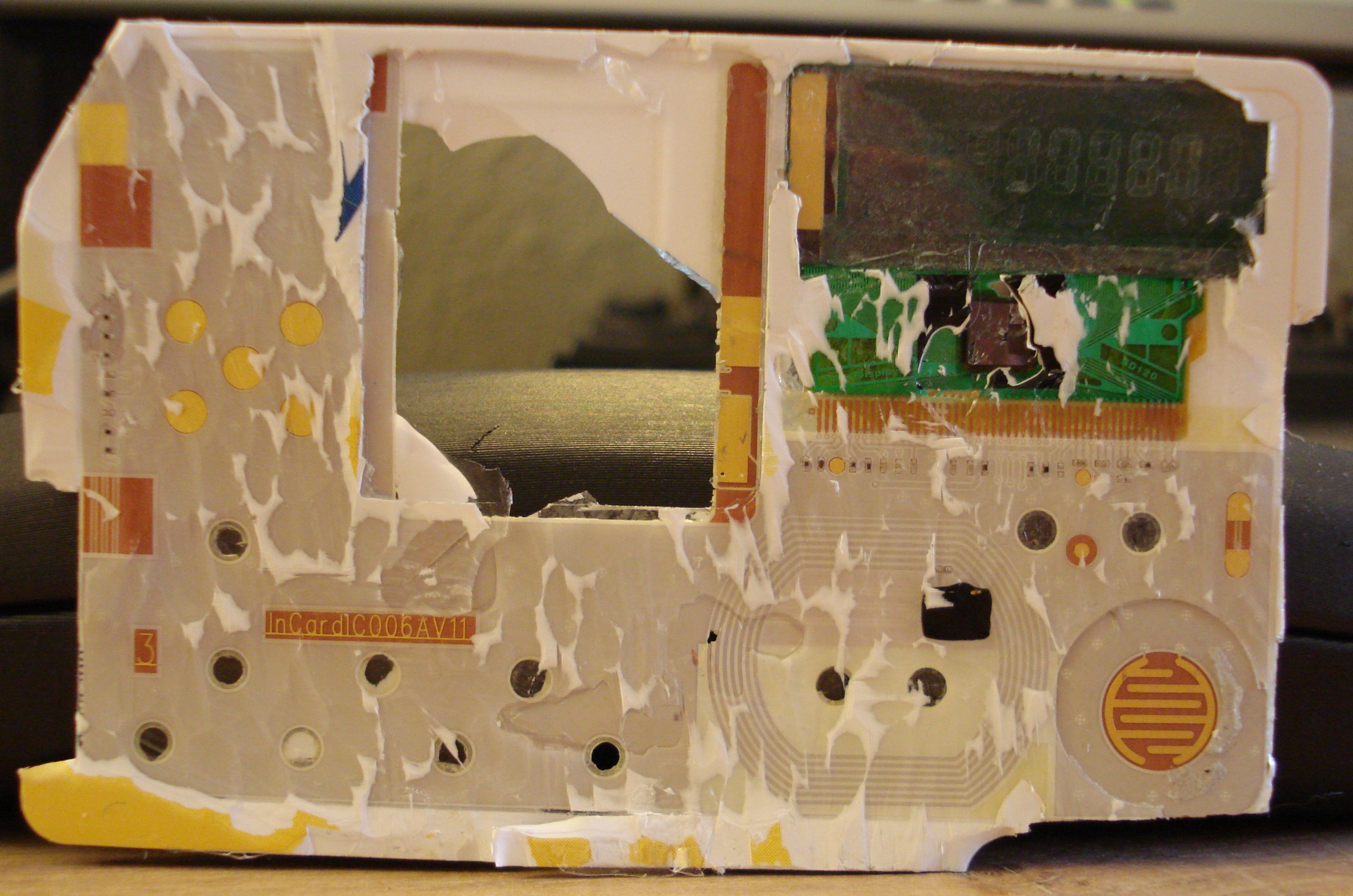
Here are my reasons:
NFC + EMV secure elements are issued by banks and can't be reprogrammed. You can't switch between them on the fly. You can only house "multiple" EMVs if you can by some grace of god magic convince the different banks, and Amex to take your card to their facility and program it with their secure info and then give it back to you.
E-ink displays are WAY thicker than they can fit in there. They are also made on GLASS substrate, much more fragile than something you want to put in your pocket. If you looks closely at the video the e-ink screen is faked by CGI. It doesn't perfectly register in the same location on every frame. There is a shake.
Driving an e-ink display requires high bias voltage, ~+/-20V. Often done via charge pumps with chips such as TI's TPS65180 (http://www.ti.com/product/tps65180). The chip alone (minus PCB) is thicker than a credit card and therefore a credit card slot. The switching capacitors you'd need to generate the voltage would also be too big to fit within that footprint.
No, I have in my pocket a PayPal Security Key: it is the same size and thickness and flexibility as a credit card, yet it houses an e-paper display: https://www.paypal-community.com/t5/image/serverpage/image-i... They have been on the market for 5+ years, so the technology is there. Plastc has a bigger display, but there is no doubt it can fit in a credit card because an e-paper display does not require that much supporting circuitry. See this guy who tore down the PayPal card: http://www.stahlke.org/dan/displaycard/
They have a full pixel display. They are different. E-Ink displays are 1.18mm thick per their spec sheet and you have to add some mechanically stiff backing to that.
Looking at a detailed photo [1] it looks like a STN segmented LCD but I could be wrong.
Incidentally, do you have a pair of callipers handy? Could you measure the PayPal Security Key?
I don't think it is the same thickness as a credit card.
I've also seen credit cards made from glass. I think they're NFC-only, though, because of the thickness, but I could be mistaken.
Only while the US still is supporting that. Once the liability shift occurs next year it'll be EMV or nothing.
1. eink can be made on flexible plastic and be very thin, and cheap too (see http://www.engadget.com/2008/09/08/esquires-e-ink-infused-ma...)
2. charge pumps can be made out of discrete components and the largest part is a coil, which can easily be laid flat and thin. You can also charge a ceramic cap (low self discharge) slowly and use it when you need to change screen contents, thus allowing you to have a smaller charge pump yet
3. PCBs can be made very thin (a cheap pcb fab I use will make 10 PCBs for $10 for me at 0.2mm thickness). And you can also make them on a flexcable that is thinner yet.
You are right about EMV though. It is supposed to be uncloneable.
2. There is no coil in a charge pump :). They use capacitors and switches. There is no inductor. For a charge pump to drive an eink like screen you need caps of about 10-20uF. I've designed about 3 different boards that drive high-res e-ink screens. You can't get those caps below 1mm at the very best.
3. Are you sure you are getting 0.2mm PCBs? That is only 8mils thick! Most standard PCBs are 62 mils ~ 1.5mm. Can you tell me who these guys are that would do super thin at prototype prices? I would want to use them (no sarcasm).
Minimum IPC thickness for 4 layer board (which is what you need for the EPSON driver to those e-inks) is 12 mils but even at that you'll have mechanical problems with that PCB. Credit card thickness FYI is 30 mils = 0.030".
What I would say to these guys is: "show me a prototype with the appropriate thickness. You have a prototype, right?"