Depending on what the community is looking to know, there may be some things we can share publicly. I’m in the software group and not intimately involved with the RE parts, but I will act as an ambassador and see if I can get the right people involved.
Throw some comments on this thread and we’ll see what we can do to help. Might be next week due to holidays.
Mostly because all the other part are already well known.
Seems like heat isn't an issue, so can they increase the clock-speed of the M1?
And will they create a larger die with 2xGPU and 2xCPUs, or will they "stitch" multiple M1 dies together on one package to have a higher yield and reduce supply chain concerns?
An M1X with 2xGPU will bring it to Radeon 5500M level which is what I have in my current 16", but still not quite to Nvidia 1080 level.
So they'll definitely need a more powerful GPU for the pro-users. I wonder if they can make a 4xGPU, or if the yield will become poor as the die size increases. Maybe they'll have to do a discrete GPU, but that doesn't seem to match their current trajectory.
And then there have been "leaks" (rumors, really) about an 32xcore M1-family CPU, but I imagine the yield of such a beast would be horrible, with all the other SOC components on the same die. Especially, if they put a 32xcore GPU on the same die.
Yield wouldn't be that bad - ARM CPUs are small in comparison to their x86 cousins. I would expect that you would get to 32 CPUs the same way everyone else does - build a 32 core design and blow enable fuses on bad CPUs, then badge as appropriate.
To get a desktop class GPU they will need to address memory bandwidth. I am assuming they are using a tile based rendering process so memory bandwidth is less of an issue in comparison to scan line rendering (do desktop GPUs still do that?) I would assume that they are enjoying the benefits of the system level cache with the CPU and GPU sharing. I would expect there to be some careful benchmarking of increasing GPU cores, memory speed, memory size and system cache size going on at Apple.
There isn't anything stopping Apple from supporting external GPUs, but it would require a new SoC with more PCIe lanes. External buses are much more power hungry and take up space on the die. I don't have a mental model of how much space plonking a PCIe x16 interconnect would cost in terms of area or power (taking into account you need to get that data across the chip too), but my gut reaction is that it isn't likely unless there is a customer use case they can't solve on chip.
They are running into their current node limits, so dont expect a 4Ghz+ coming unless they decide to remake the whole thing in High Performance Node. ( Which means it will cost a lot more for a relatively niche volume.)
>I wonder if they can make a 4xGPU
GPU increase should be given, and die size / yield would not be a concern / problem. The question is how will they handle the additional memory bandwidth requirement? As you can see in the Die-Shots those DDR I/O side are already take up much of the side space. Going with HBM2? Or LPDDR5?
>32xcore M1-family CPU, but I imagine the yield of such a beast would be horrible,
A 32x CPU / GPU Core M1 will only be 4x increase from its current form. If you exclude I/O part, the CPU + GPU + Cache is only a little more than 50% of die size, or ~60mm2. 4x That is only 240mm2+. The final product would be a sub 350mm2 if you include all the additional. Which is roughly inline with the current estimate of AWS Graviton 2 die size ( ~400mm2).
But yes, M1 ( A14X ) isn't really that interesting. The most exciting part is how they will go about doing high performance chip. Especially on iMac and Mac Pro.
And doubling the M1-GPU will not be enough to even surpass current Macbook Pro offerings. So they'll also need to do something more on that front.
Archive.org seems to work:
https://web.archive.org/web/20201227010504/https://www.techi...
How far can someone with time and money go towards reverse engineering a chip from such pictures?
Identifying the GPU, for example, is based on recognizing that there are eight repeated elements within it, and matching that with the known fact that there are eight GPU cores.
Infrared camera
I/O controllers, various PHYs, the display pipeline and the media engine account for a significant fraction of chip.
We also know the M1 has an integrated SSD controller, ISP and Thunderbolt which probably take a good chunk of room too.
[1] https://potatopc.net/amd-renoir-die-annotation-raises-hopes-...
SSD controller and even Thunderbolt. That's the most integrated SoC I've heard of.
The Secure Enclave is a good one to point out that is in the unlabeled space.
Certainly some non-DDR peripherals are in the unlabeled space, but it would be neat to have a more comprehensively labeled diagram. I wouldn't expect most peripherals to take up so many transistors compared to the processor cores.
EDIT: the name Bionic has been used since the A11 when the Neural Engine was introduced. Fusion introduced big.LITTLE.
For example, in the layout to the right of the DDR on the M1, it looks like some significant optimization was done, but only in certain areas.
It is used by the GPU, neural engines,... in addition to the CPU itself.
They’re hugely powerful general purpose computing devices - many people’s primary computing device if you go outside the tech bubble. They do compute intensive tasks like photo manipulation, on-line video editing, grading, and compression, they do face detection, depth estimation, etc etc.
I don’t know why people still say ‘wow all this for a telephone’ like all it does is make analog phone calls.
iPhone
As an aside, I was wondering what things does the iPhone 12 do that can even begin to tax all this horespower?
This just sounds like "DAE think phone=bad XD" anti-intellectualism.
> A DFR report will be available to TechInsights subscribers on Apple's M1 disruptive chip architecture in January 2021.
So I assume the actual write-up is still a work-in-progress. Perhaps we just need to be patient and come back a month later.
The are more than just a document. A DFR includes in depth analysis, hundreds of supporting images, and usually access to the Circuit Vision for it. CV is a viewer that allows drilling into the chip down to viewing individual transistors along with the chip schematics. Think map tiles but for a chip.
Disclosure: I work at TechInsights.
A die shot that Apple themselves showed at the event. Which has had the same level of annotations previously by Anantech.
Sure, the DFR in early 2021 will be much more detailed, but also expensive to the point 0.001% of HN viewers will actually be able to see it. As such, I think your skepticism of this being worthy of home page billing is not out of line.
For the record, this is not meant to be a dig at TechInsights. I’ve seen a DFR before and they really are good for what they are, it’s just not something most HNers would gain value from, even if it were free.
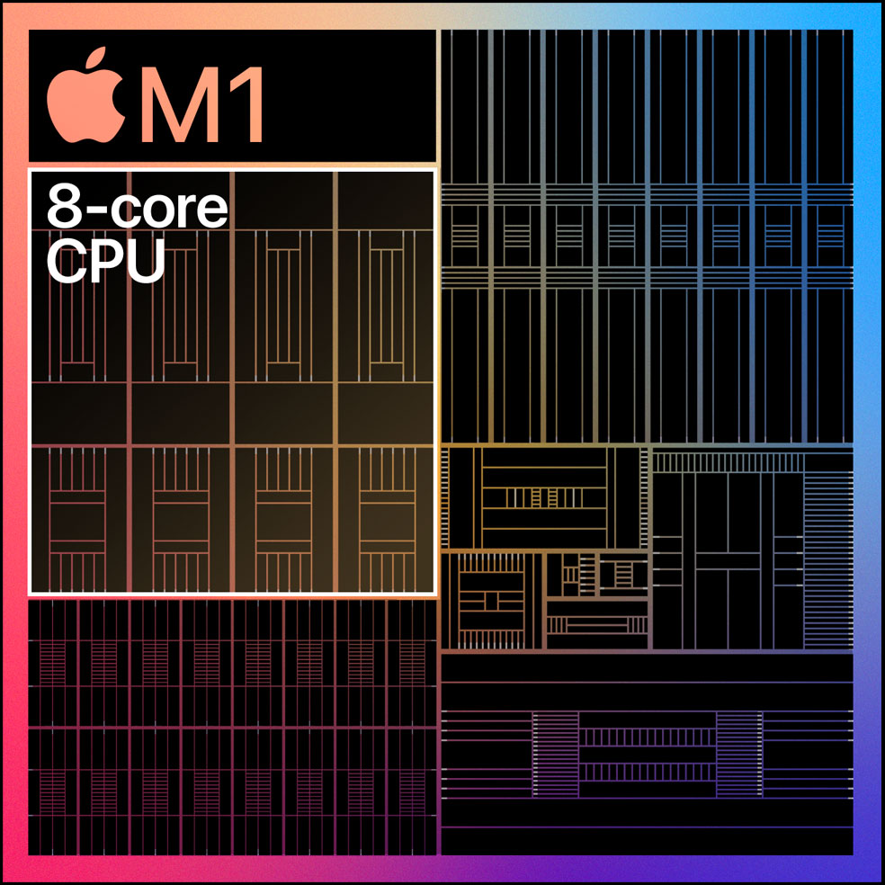
[1] https://www.apple.com/v/mac/m1/a/images/overview/chip_cpu__d...
I'm a rather technical folk and even I don't care.
The graphics they put on slides or marketing sites aren’t supposed to be technical reference material, usually it’s just about conveying the idea of a SoC or performance improvements, or relative sizes, or whatever.
You don't need to see the cartoonized version of it either. May be its easier as a schematic to explain? Not sure. A list of M1's features would work equally well. I think its just marketing pizzaz.
A quick visual comparison shows this to be pretty accurate, just inverted and rotated.